KOR
Company
CEO Message Overview & Values History Sites & Affiliates
Products
AlN Heater SiC Heater Film Heater Ceramic Heater Printed Electronics
Technology
Heater Design Manufacturing Certifications & Patents
Contact
Location Request a Quote
Home · Technology

Technology & Quality

We design with thermal simulation, laser-trim resistance to target and control it to 3σ. Design values that become product performance — that is the basis of BH SEMICON quality.

Core Competence

Designed by simulation,
tuned by laser

The two pillars of BH SEMICON heater quality: in-house design based on thermal simulation and fine resistance control by laser trimming. We manage everything by the numbers, from start to finish, so design values become product performance.

HighTargetLow ΔT-based design ● Heat loss at pins/holes → offset by circuit density
01 · Thermal Simulation

In-house design based on thermal simulation

We convert the temperature distribution your process requires into an analysis model and optimize each zone's power density and circuit line width by simulation. Because temperature uniformity (ΔT) is predicted before prototyping, we reach the target performance with the first design, without trial and error.

  • In-house analysis process converting the required temperature distribution into power-density design
  • Local heat loss from lift pins, holes and cooling structures compensated in advance by circuit density
  • Zone layout and boundaries for 1 to 15+ zones determined by analysis
  • Analysis model continuously refined by comparing simulation results with measured temperatures
Segment1 / 3
TARGET12.50 Ω
MEASURED11.72 Ω
POSITIONING
02 · Laser Trimming & 3σ Control

Laser trimming · 3σ fine resistance control

We run a trimming process that measures each segment's resistance in real time while laser-trimming it precisely to target. We finely control resistance deviation by zone and segment, and manage resistance data for every unit statistically to 3σ, reproducing temperature uniformity in every product.

  • Closed-loop process: measure → trim → re-measure until resistance converges on target
  • Fine control of resistance deviation by zone and segment for uniform power density
  • Resistance data logged for every unit · ±3σ statistical process control (SPC)
  • Simulated design values match actual resistance → design performance delivered as-is
01Required temperature distribution
02Thermal simulation design
03Circuit forming (plating · printing)
04Laser trimming to target resistance
053σ statistical control · shipment
Design Capability

Heater Design

A heater's performance is decided not by its material but by its circuit design. Converting the required temperature distribution into power density and realizing it as an ultra-fine circuit pattern is BH SEMICON's core technology. We design without limits: 1 to 15+ zones, 110–400℃ operating temperature and 2T–4T plate thickness.

1 ZoneSingle zone
2 8 15
15 Zone +High-density multi-zone

From a single zone to high-density layouts of 15+ zones — we design and build any zone count, shape and power density your specification requires.

Production examples — 2 · 8 · 15 zones

2 Zone

A standard layout with independent inner and outer control for baseline temperature uniformity.

8 Zone

A precision layout split by both radius and angle to compensate even local heat loss caused by the equipment structure.

15 Zone +

A high-density layout with fine-grained control across the wafer. In mass production with both plating and printing processes; we also design and build 15+ zones.

Measured Uniformity · 15-zone measurement

Temperature uniformity,
proven to 0.01℃

≤ 0.04℃Temperature variation across the wafer
(within ±0.02℃)
≤ 0.05℃Temperature standard deviation σ

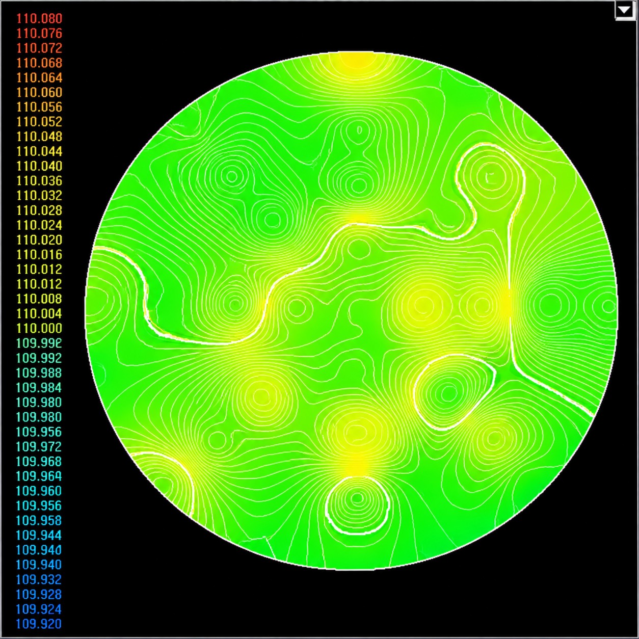
With a 15-zone heater, the measured temperature across the wafer stays within ±0.02℃ of the set point. Max–min difference ≤ 0.04℃, standard deviation σ ≤ 0.05℃ — built to meet the uniformity spec (σ<0.05℃) required for Soft Bake and PEB on lithography tracks.

※ Measured on a 15-zone heater in KrF equipment — Soft Bake · PEB (100℃) σ 0.041–0.049℃ / spec σ<0.05℃

Measured temperature map of a 15-zone heater: at a 110℃ set point the whole wafer falls evenly within the green-yellow band around 110℃

Ultra-fine circuit forming

Korea's only ultra-fine circuit forming technology finely controls circuit line width and spacing. Power density can be distributed freely by position, so even complex temperature profiles can be met through circuit design alone.

Verified temperature uniformity

We verify temperature uniformity through repeated cycles of design, prototyping, measurement and correction. High-quality temperature uniformity and durability, from low- to high-temperature products, are the secret behind 20 years of mass production.

Dual Process

Plating and printing: two strengths

BH SEMICON has developed both processes for forming heating circuits in-house, and applies the best one for your required temperature and precision.

Plating

Plating process

Forms circuits on the ceramic surface by plating. Its strength is precise circuitry; it is used in AlN Heater mass production.

StrengthsFine-circuit precision, uniform conductor thickness
Printing

Printing process

Forms circuits by printing and firing heating-element paste. Its strength is higher operating temperature; it is used in AlN Heater mass production.

StrengthsHigh-temperature capability, multilayer and complex patterns
Printed Electronics

From printing technology to electronic components

We have extended the fine-pattern technology built up in printing heater circuits to PET · Ag printed electronic components. We achieve fine patterns down to 100µm by printing and apply them to capacitive touch sensors and more.

Printing Technology · Fine Pattern

Fine patterns down to 100µm,
by printing

100µmMinimum line width
achieved by printing

We print silver (Ag) paste on PET film to form electrode patterns. Even by printing, we can achieve fine patterns down to 100µm in width, and the fine-pattern technology refined in printing heater circuits keeps line width and thickness consistent.

  • Ag paste printing
  • 100µm fine patterns
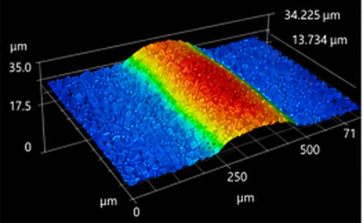
  • 3D profile measurement
3D surface profile measurement of a printed Ag line raised on PET
3D surface profile of a printed Ag line (height scale 0–35µm)
How it works

How a capacitive touch sensor works

When a finger touches the surface: capacitance changes → the touch is detected → the controller performs signal processing

Before touchBaseline capacitance
ΔC change
On touchCapacitance changes
Signal processingTouch · gesture recognition

View Printed Electronics products

Manufacturing Process

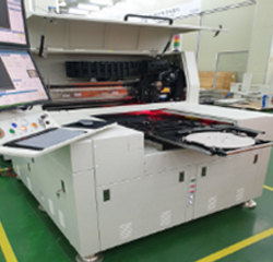
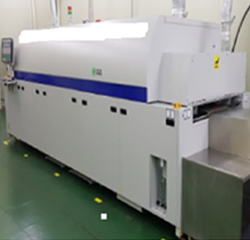
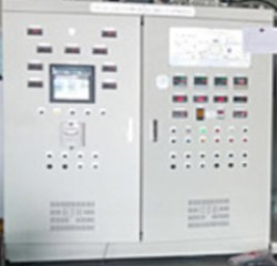
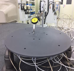
11-step in-house production process

Every step, from pretreatment to final inspection, is completed in-house. With no transfers between processes, quality variation is low, and lead time and confidentiality benefit too.

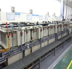
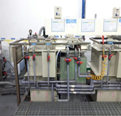
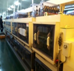
Pretreatment equipment
01Pretreatment
Plating line
02Plating line
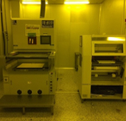
Circuit forming process
03Circuit forming
Circuit inspection
04Circuit inspection
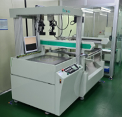
Printing process
05Printing
O/G printing process
06O/G printing
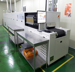
Heat treatment equipment
07Heat treatment
Laser trimming equipment
08Laser trimming
Soldering process
09Soldering
Brazing process
10Brazing
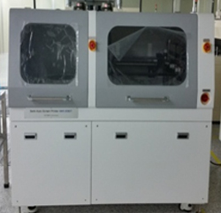
Assembly and final inspection
11Assembly · final inspection
100%

100% inspection
before every shipment

Certification & Patent

Certifications & Patents

ISO 9001

International quality management system certification (DAS, obtained 2006)

AlN Heater manufacturing patent

Patents filed and held for AlN Heater manufacturing methods (2015–)

View all certificates and patents (Korean)

Have a technical question?

Tell us your process conditions and we'll share our design review.

Technical inquiry